

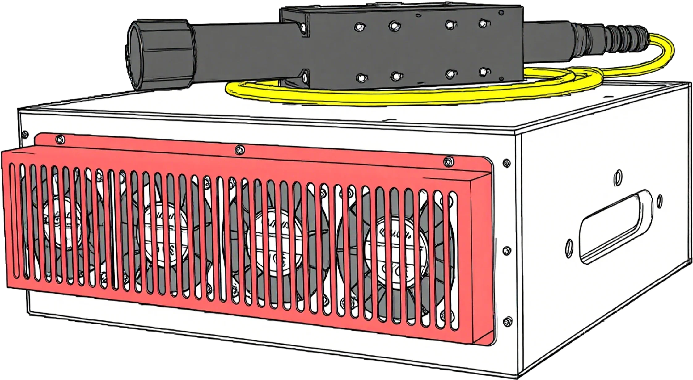
Laser Source
Laser Source
Pulsed Fiber Laser
UV Laser
Ultrafast Laser
CO2 Laser
CW Fiber Laser
QCW Fiber Laser
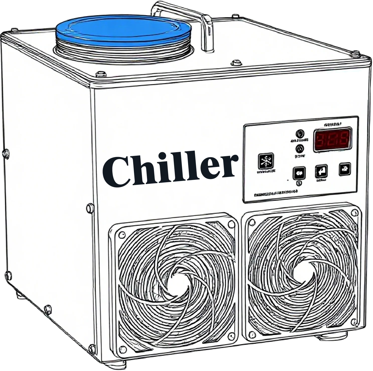
Chiller
Chiller
Air Conditioner
Optics
Optics
Scan Head
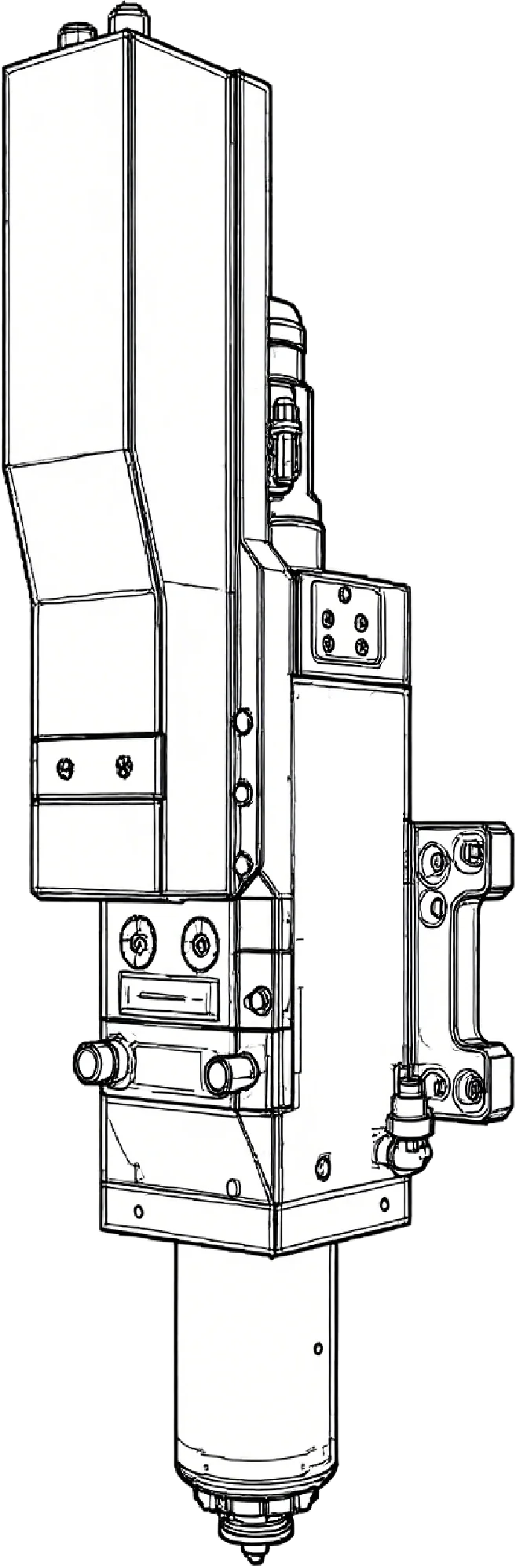
Cutting Head
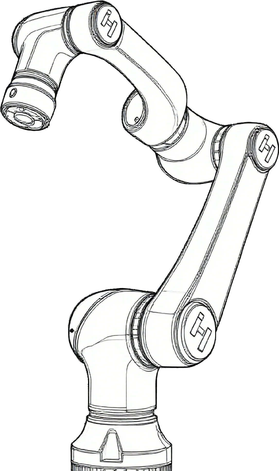
Robot
Robot
Collaborative Robot
Motion Control
Motion Control
Ball Screws
Liner Guide
Motion Stage
Linear Motor
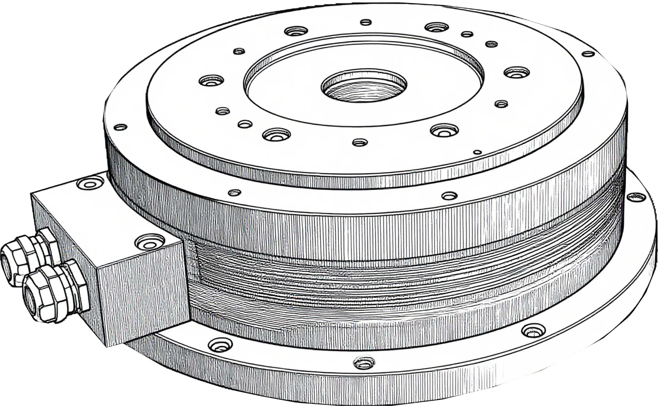
Torque Motor
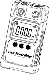
Laser Power Meter
Laser Power Meter
Laser Power Meter


- Home
- Product +
- Application +
- Solutions +
- Service Support +
- About Us +
- News +
- Contact Us +